At EMiL, we provide state-of-the-art electron microscopy and microanalysis services, empowering groundbreaking research and industrial innovations. Whether you are from academia, the private sector, or federal agencies, our cutting-edge facility is ready to support your materials science needs.
For project advice, consultations, additional information, or to schedule a session, please email Dr. Melissa Drignon at melissa.drignon@unlv.edu.
Our Services
Explore a comprehensive range of advanced tools and services tailored to meet your research and industrial requirements:
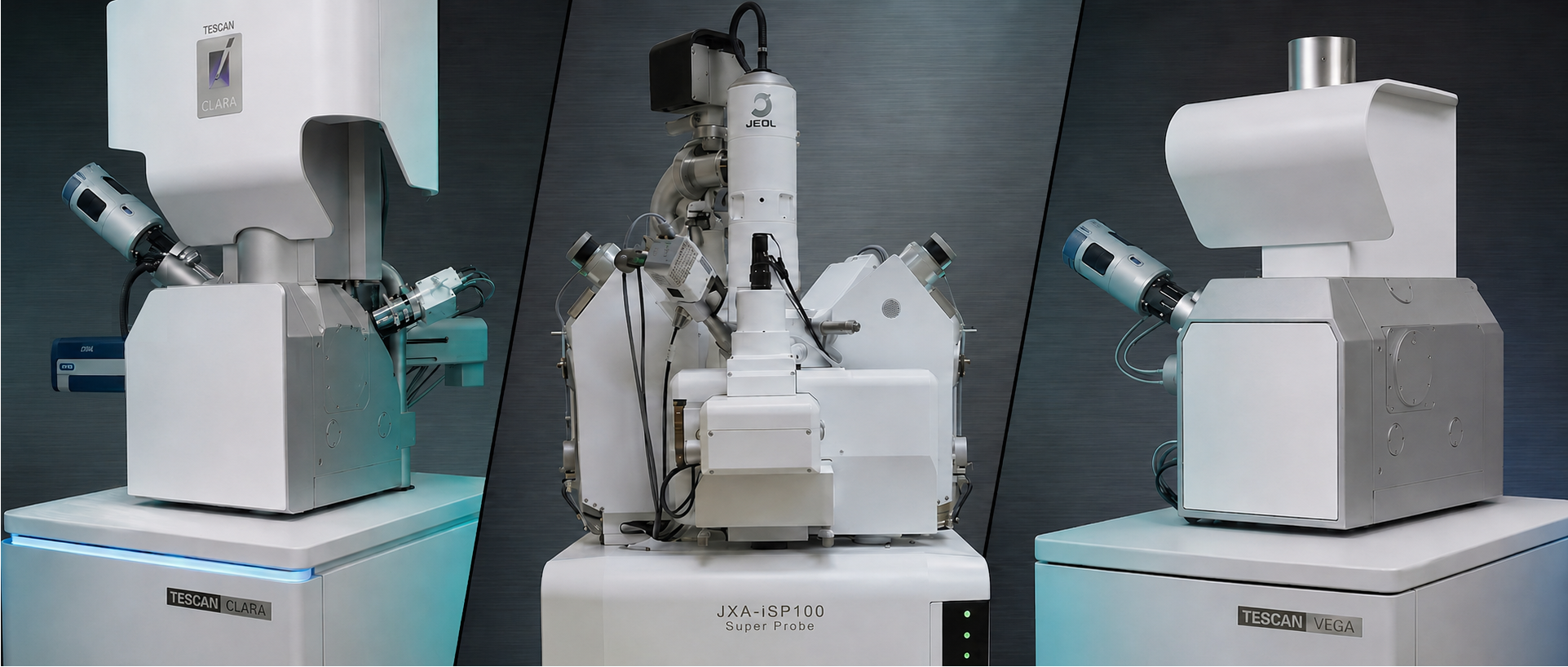
- High-Resolution Imaging: Capture detailed images with precision using our Scanning Electron Microscopes (SEMs), including the newly installed TESCAN VEGA and field-emission TESCAN CLARA. Our advanced imaging techniques allow you to visualize your samples at both the micron and nanoscale, providing essential insights into their structure and morphology. Capabilities include high-resolution imaging in Secondary Electron (SE), Backscatter Electron (BSE), Scanning Transmission Electron Microscopy (STEM), and Cathodoluminescence (CL) modes.
- Elemental and Chemical Analysis: Identify and quantify the composition of your samples with our advanced analytical techniques. Our Energy-Dispersive Spectroscopy (EDS) offers quick and precise elemental analysis, while Electron Backscatter Diffraction (EBSD) provides insights into crystallographic orientation and phase distribution, essential for comprehensive material characterization. Enhance your capabilities with our newly delivered JEOL JXA-ISP 100 Electron Probe Microanalyzer, which delivers high spatial resolution and analytical precision for quantitative analyses across all naturally occurring elements (except H, He, and Li) with low detection limits.
- Data Interpretation and Support: Support is available for analyzing and interpreting your data for publication or production insights, ensuring maximum value is derived from your research efforts.
Techniques and Services Include:
Scanning Electron Microscopy (SEM) capabilities
- Micron- and nano-scale particle imaging
- Elemental X-ray mapping (EDS)
- Phase identification using EDS and electron backscatter diffraction (EBSD)
- EBSD imaging and analysis
- Cathodoluminescence (CL) imaging
- Environmental SEM (ESEM) imaging of non-conductive and/or uncoated samples in low-vacuum mode
- Scanning transmission electron microscopy (STEM-in-SEM) imaging
Electron Probe Microanalyzer (EPMA) – JEOL JXA ISP 100
- High-precision quantitative elemental analyses are performed using wavelength-dispersive spectroscopy (WDS), including spot analyses, and elemental mapping for major, minor, and trace elements.
Comprehensive Sample Preparation
Equipment is available for polishing and sputter coating, including a PACE Technologies vibratory polisher, ensuring high-quality sample preparation for electron microscopy and EBSD analysis.
Collaborative Research Environment
EMiL supports groundbreaking research across diverse fields. Current users include researchers in geoscience, chemistry, biochemistry, engineering, physics, life sciences, materials science, and the mining industry, demonstrating the facility’s capability to serve a wide range of scientific disciplines.
Lab Personnel
- Dr. Melissa Drignon – Facility Manager
melissa.drignon@unlv.edu - Prof. Pamela Burnley – Co-Faculty Director
pamela.burnley@unlv.edu - Dr. Andrew Martin – Co-Faculty Director
andrew.martin@unlv.edu - Prof. Arya Udry – Co-Faculty Director
arya.udry@unlv.edu
Location
Electron Microanalysis & Imaging Laboratory (EMiL)
Science and Engineering Building SEB
University of Nevada Las Vegas Box 454022
4505 S. Maryland Parkway
Las Vegas NV 89154-4010
For more details on the principles and applications of SEM and EPMA, visit here.
Advanced Materials Research and Imaging Services for Academia, Industry, and Government

