Electron Beam Interactions and Analytical Signals
Scanning electron microscopes (SEM) and electron probe microanalyzers (EPMA) generate a variety of signals when a focused electron beam interacts with a specimen. These signals—including electrons, visible light (photons), and characteristic X-rays—provide information about surface morphology, crystal structure, and chemical composition. The signal selected determines the imaging or analytical technique being performed.
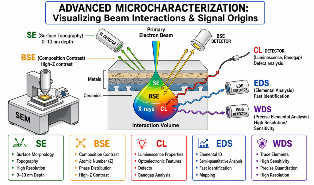
Electron Beam Signals and Imaging Techniques
- Secondary Electron (SE) Imaging: Secondary electrons are emitted from the near-surface region of a specimen during electron beam interaction. Because they originate from only a few nanometers below the surface, they provide high-resolution images of surface morphology and topography.
- Backscattered Electron (BSE) Imaging: Backscattered electrons are elastically scattered from deeper within the specimen. Their intensity increases with average atomic number (Z), producing compositional contrast in which higher atomic number phases appear brighter than lower atomic number phases.
- Cathodoluminescence (CL) Imaging: Cathodoluminescence imaging detects visible light emitted from a sample when it is bombarded by an electron beam. CL is particularly useful for studying mineral growth histories, zoning patterns, dissolution, deformation, and crystallographic characteristics. It can also reveal variations caused by impurities, defects, and structural features within minerals.
X-ray-Based Chemical Analysis
Energy-Dispersive Spectroscopy (EDS)
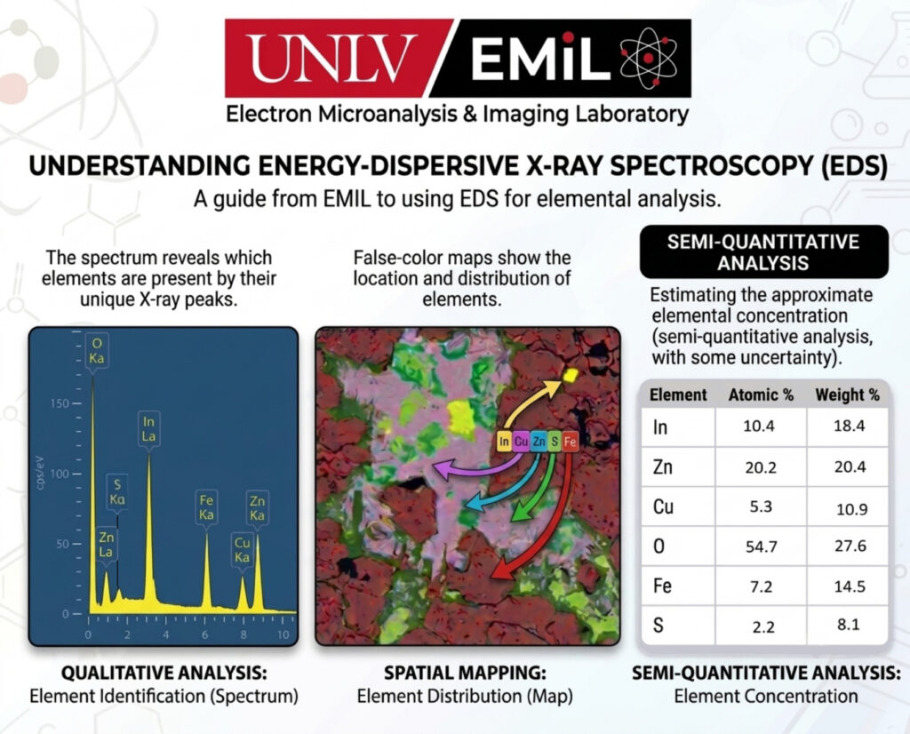
EDS measures characteristic X-rays produced when a sample is bombarded by an electron beam. The detector measures the energy of emitted X-rays, allowing rapid identification and semi-quantitative analysis of the elements present.
EDS can be performed on both SEM and EPMA instruments and is commonly used for mineral identification and elemental distribution studies. Data can be collected as:
- Point analyses: determine the composition of individual phases or specific locations.
- Line scans: measure changes in elemental concentrations along a selected path.
- Elemental maps: visualize the spatial distribution of elements throughout an area.
EDS provides fast chemical characterization but generally has lower spectral resolution and detection limits compared to WDS.
Wavelength-Dispersive Spectroscopy (WDS)
WDS is an analytical technique performed primarily on electron microprobes (EPMA) that measures characteristic X-rays emitted from a sample during electron bombardment. Unlike EDS, WDS uses diffraction crystals to separate X-rays based on wavelength, providing higher spectral resolution and lower detection limits.
WDS enables accurate quantitative analysis of major, minor, and trace elements within mineral phases. Analyses can be collected as:
- Point analyses: quantitative measurements of specific mineral phases.
- Elemental maps: high-resolution visualization of elemental zoning and compositional variations.
Because of its high precision and sensitivity, WDS is widely used for quantitative mineral chemistry, trace element analysis, and detailed compositional mapping.
Electron Backscatter Diffraction (EBSD)
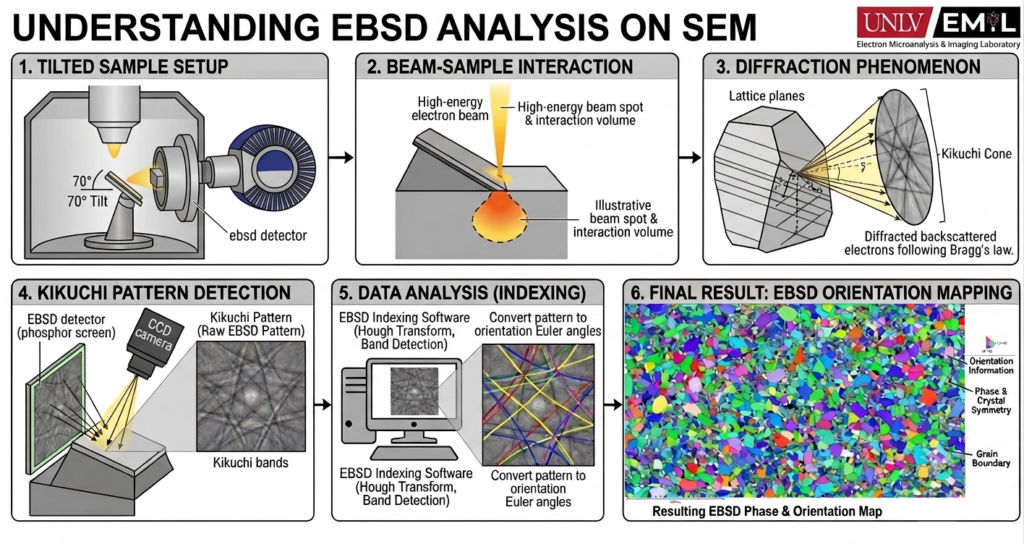
EBSD analyzes crystallographic orientation and microstructural characteristics of materials. Electron diffraction patterns generated from the sample surface provide information about grain orientation, grain boundaries, deformation textures, and crystallographic relationships.
Scanning Electron Microscope (SEM)
Scanning Electron Microscopy (SEM) is a versatile technique that combines high-resolution imaging with analytical capabilities to characterize the morphology, composition, and crystallography of materials. By integrating detectors such as SE, BSE, EDS, EBSD, and, on some systems, WDS, SEM provides comprehensive information about a specimen’s surface and microstructure for research, quality control, and failure analysis.
Electron microprobe microanalyzer (EPMA)
Electron Probe Microanalyzer (EPMA) is a specialized electron microscopy technique designed for highly accurate quantitative chemical analysis. In addition to SEM imaging capabilities, EPMA uses multiple wavelength-dispersive spectrometers (WDS), energy-dispersive spectroscopy (EDS), and optical microscopy to determine elemental concentrations with micron-scale spatial resolution.
EPMA requires a highly polished sample surface, typically with a surface finish better than 1 µm. Non-conductive samples may require a thin conductive coating to optimize analytical performance and minimize charging.
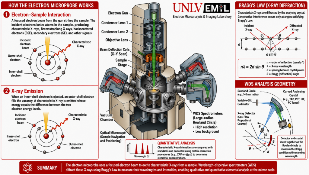
How WDS works in EPMA
When the electron beam interacts with a sample, inner-shell electrons may be ejected through inelastic collisions, creating vacancies in the atom. As higher-energy electrons fill these vacancies, characteristic X-rays are emitted. Because each element produces X-rays with unique wavelengths, these emissions can be used to identify and quantify the elemental composition.
Wavelength-dispersive spectroscopy (WDS) separates characteristic X-rays according to their wavelength using analyzing crystals and detectors. Based on Bragg’s Law, only X-rays with specific wavelengths are diffracted by the crystal into the detector at a given angle, enabling highly precise elemental measurements.
Bragg’s Law:
Where:
- n = diffraction order (1, 2, 3, …)
- λ = X-ray wavelength
- d = crystal spacing
- θ = incident angle
By comparing measured X-ray intensities with those from well-characterized standards, EPMA provides highly accurate quantitative chemical analyses. Depending on the element, concentration, counting time, and analytical conditions, detection limits can reach the parts-per-million (ppm) range.
Advantages of EPMA
- Quantitative elemental analysis at the micron scale
- Higher accuracy, precision, and spectral resolution than EDS
- Analysis of major, minor, and trace elements
- High-resolution elemental mapping and chemical zoning studies
- Non-destructive, in situ chemical analysis
- Analysis of features as small as approximately 1 µm
- Detection of nearly all elements, except hydrogen (H) and helium (He)
Applications of SEM and EPMA
SEM and EPMA are widely used in scientific research and industry, including:
- Geology and mineral exploration
- Materials science and engineering
- Semiconductor research
- Electronics manufacturing
- Failure analysis and quality control
- Metallurgy and alloy characterization
- Construction materials
- Biological and chemical research
These techniques enable researchers and industry professionals to investigate material composition, microstructures, textures, defects, and elemental distributions with exceptional spatial resolution.
